We looked at the circuit of a simple autonomous charger for mobile equipment, working on the principle of a simple stabilizer with lowering battery voltage. This time we will try to assemble a slightly more complex, but more convenient memory. The batteries built into miniature mobile multimedia devices usually have a small capacity, and, as a rule, are designed to play audio recordings for no more than several tens of hours when the display is turned off, or to play several hours of video or several hours of reading e-books. If a power outlet is unavailable or the power supply is turned off for a long period of time due to bad weather or other reasons, then various mobile devices with color displays will have to be powered from built-in energy sources.
Given that such devices consume considerable current, their batteries may be discharged before electricity is available from a wall outlet. If you do not want to immerse yourself in primitive silence and peace of mind, then to power your handheld devices, you can provide a backup autonomous energy source, which will help out both during a long journey into the wild, and in case of man-made or natural disasters, when your settlement may be on the verge of destruction. several days or weeks without power supply.

Mobile charger circuit without 220V network
The device is a linear voltage stabilizer of the compensation type with a low saturation voltage and a very low intrinsic current consumption. The energy source for this stabilizer can be a simple battery, rechargeable battery, solar or manual electric generator. The current consumed by the stabilizer when the load is off is about 0.2 mA at an input supply voltage of 6 V or 0.22 mA at a supply voltage of 9 V. The minimum difference between the input and output voltage is less than 0.2 V at a load current of 1 A! When the input supply voltage changes from 5.5 to 15 V, the output voltage changes by no more than 10 mV at a load current of 250 mA. When the load current changes from 0 to 1 A, the output voltage changes by no more than 100 mV at an input voltage of 6 V and by no more than 20 mV at an input supply voltage of 9 V.
A self-resetting fuse protects the stabilizer and battery from overload. The reverse-connected diode VD1 protects the device from reverse polarity of the supply voltage. As the supply voltage increases, the output voltage also tends to increase. To maintain the output voltage stable, a control unit assembled at VT1, VT4 is used.
An ultra-bright blue LED is used as a reference voltage source, which, while performing the function of a micro-power zener diode, is an indicator of the presence of output voltage. When the output voltage tends to increase, the current through the LED increases, the current through the emitter junction VT4 also increases, and this transistor opens more, and VT1 also opens more. which bypasses the gate-source of the powerful field-effect transistor VT3.
As a result, the resistance of the open channel of the field-effect transistor increases and the voltage across the load decreases. Trimmer resistor R5 can be used to adjust the output voltage. Capacitor C2 is designed to suppress self-excitation of the stabilizer as the load current increases. Capacitors C1 and SZ are blocking capacitors in the power supply circuits. Transistor VT2 is included as a micro-power zener diode with a stabilization voltage of 8..9 V. It is designed to protect against breakdown of the VT3 gate insulation by high voltage. A gate-source voltage that is dangerous for VT3 may appear when the power is turned on or due to touching the terminals of this transistor.
Details. The KD243A diode can be replaced by any of the KD212, KD243 series. KD243, KD257, 1N4001..1N4007. Instead of KT3102G transistors, any similar ones with low reverse collector current are suitable, for example, any of the KT3102, KT6111, SS9014, BC547, 2SC1845 series. Instead of the KT3107G transistor, any of the KT3107, KT6112, SS9015, VS556, 2SA992 series will do. A powerful p-channel field-effect transistor of the IRLZ44 type in a TO-220 package, has a low gate-source opening threshold voltage, a maximum operating voltage of 60 V. The maximum direct current is up to 50 A, the open channel resistance is 0.028 Ohm. In this design, it can be replaced with IRLZ44S, IRFL405, IRLL2705, IRLR120N, IRL530NC, IRL530N. The field-effect transistor is installed on a heat sink with a cooling surface area sufficient for a particular application. During installation, the terminals of the field-effect transistor are short-circuited with a jumper wire.

The autonomous charger can be mounted on a small printed circuit board. As an autonomous power source, you can use, for example, four pieces of series-connected alkaline galvanic cells with a capacity of 4 A/H (RL14, RL20). This option is preferable if you plan to use this design relatively rarely.

If you plan to use this device relatively often or your player consumes significantly more current even when the display is off, then it would be advisable to use a 6 V rechargeable battery, for example, a sealed motorcycle battery or from a large hand-held flashlight. You can also use a battery of 5 or 6 nickel-cadmium batteries connected in series. When hiking, fishing, to recharge batteries and power a handheld device, it may be convenient to use a solar battery capable of delivering a current of at least 0.2 A with an output voltage of 6 V. When powering the player from this stabilized energy source, it should be taken into account that the regulating transistor is turned on into the negative circuit, therefore, simultaneous power supply of the player and, for example, a small active speaker system is only possible if both devices are connected to the output of the stabilizer.
The purpose of this circuit is to prevent a critical discharge of the lithium battery. The indicator turns on the red LED when the battery voltage drops to a threshold value. The LED turn-on voltage is set to 3.2V.

The zener diode must have a stabilization voltage lower than the desired LED turn-on voltage. The chip used was 74HC04. Setting up the display unit involves selecting the threshold for turning on the LED using R2. The 74NC04 chip makes the LED light up when the discharge reaches the threshold that will be set by the trimmer. The current consumption of the device is 2 mA, and the LED itself will light up only at the moment of discharge, which is convenient. I found these 74NC04 on old motherboards, so I used them.
Printed circuit board:


To simplify the design, this discharge indicator may not be installed, because the SMD chip may not be found. Therefore, the scarf is specially placed on the side and can be cut along the line, and later, if necessary, added separately. In the future I wanted to put an indicator on the TL431 there, as a more profitable option in terms of details. The field-effect transistor is available with a reserve for different loads and without a radiator, although I think it is possible to install weaker analogues, but with a radiator.


SMD resistors are installed for SAMSUNG devices (smartphones, tablets, etc., they have their own charging algorithm, and I do everything with a reserve for the future) and they can not be installed at all. Do not install domestic KT3102 and KT3107 and their analogues; the voltage on these transistors was floating due to h21. Take BC547-BC557, that's it. Source of the diagram: Butov A. Radio constructor. 2009. Assembly and adjustment: Igoran .
Discuss the article MOBILE CHARGING FOR YOUR PHONE
I wonder what the Siemens charger (power supply) consists of and whether it is possible to repair it yourself in the event of a breakdown.
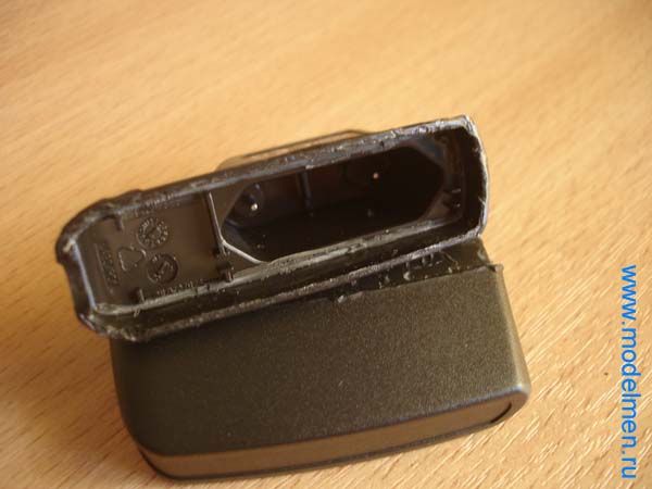
First, the block needs to be disassembled. Judging by the seams on the body, this unit is not intended for disassembly, therefore it is a disposable item and you don’t have to place much hope in the event of a breakdown.

I literally had to tear apart the body of the charger; it consists of two tightly glued parts.

Inside is a primitive circuit board and several parts. The interesting thing is that the board is not soldered to the 220V plug, but is attached to it using a pair of contacts. In rare cases, these contacts may oxidize and lose contact, leaving you thinking the unit is broken. But I was pleasantly pleased with the thickness of the wires going to the connector for the mobile phone; you don’t often see a normal wire in disposable devices; usually it is so thin that it’s scary to even touch it).

There were several parts on the back of the board; the circuit turned out to be not so simple, but still not so complicated that you couldn’t fix it yourself.

Below in the photo are the contacts of the inside of the case.
There is no step-down transformer in the charger circuit; its role is played by an ordinary resistor. Next, as usual, a couple of rectifying diodes, a pair of capacitors for rectifying the current, then comes a choke and finally a zener diode with a capacitor completes the chain and outputs the reduced voltage to a wire with a connector to the mobile phone.

The connector has only two contacts.

I present another device from the “Don’t Take!” series.
The kit includes a simple microUSB cable, which I will test separately with a bunch of other cords.
I ordered this charger out of curiosity, knowing that in such a compact case it is extremely difficult to make a reliable and safe 5V 1A mains power device. The reality turned out to be harsh...
It came in a standard bag with bubble wrap.
The case is glossy, wrapped in protective film.
Overall dimensions with plug 65x34x14mm 


The charger immediately turned out to be inoperative - a good start...
At first, the device had to be disassembled and repaired in order to be able to test it.
It is very easy to disassemble - on the latches of the plug itself.
The defect was discovered immediately - one of the wires to the plug fell off, the soldering turned out to be of poor quality. 
The second soldering is no better 
The installation of the board itself was done normally (for the Chinese), the soldering was good, the board was washed. 


Real device diagram 
What problems were found:
- Quite weak attachment of the fork to the body. The possibility of her remaining disconnected from the socket is not excluded.
- Lack of input fuse. Apparently those same wires to the plug are the protection.
- Half-wave input rectifier - unjustified savings on diodes.
- Small capacitance of the input capacitor (2.2 µF/400V). The capacity is clearly insufficient for the operation of a half-wave rectifier, which will lead to increased voltage ripple across it at a frequency of 50 Hz and to a decrease in its service life.
- Lack of input and output filters. Not a big loss for such a small and low-power device.
- The simplest converter circuit using one weak transistor MJE13001.
- A simple ceramic capacitor 1nF/1kV in the noise suppression circuit (shown separately in the photo). This is a gross violation of device security. The capacitor must be of at least Y2 class.
- There is no damper circuit for suppressing reverse emissions of the primary winding of the transformer. This impulse often breaks through the power key element when it heats up.
- Lack of protection against overheating, overload, short circuit, and increased output voltage.
- The overall power of the transformer clearly does not reach 5W, and its very miniature size casts doubt on the presence of normal insulation between the windings.
Now testing.
Because The device is not inherently safe; the connection was made through an additional mains fuse. If something happens, at least it won’t burn you and won’t leave you without light.
I checked it without the housing so that I could control the temperature of the elements.
Output voltage without load 5.25V
Power consumption without load less than 0.1 W
Under a load of 0.3A or less, charging works quite adequately, the voltage maintains a normal 5.25V, the output ripple is insignificant, the key transistor heats up within normal limits.
Under a load of 0.4A, the voltage begins to fluctuate slightly in the range of 5.18V - 5.29V, the ripple at the output is 50Hz 75mV, the key transistor heats up within normal limits.
Under a load of 0.45A, the voltage begins to noticeably fluctuate in the range of 5.08V - 5.29V, the ripple at the output is 50Hz 85mV, the key transistor begins to slowly overheat (burns your finger), the transformer is lukewarm.
Under a load of 0.50A, the voltage begins to fluctuate greatly in the range of 4.65V - 5.25V, the ripple at the output is 50Hz 200mV, the key transistor is overheated, the transformer is also quite hot.
Under a load of 0.55A, the voltage jumps wildly in the range of 4.20V - 5.20V, the ripple at the output is 50Hz 420mV, the key transistor is overheated, the transformer is also quite hot.
With an even greater increase in load, the voltage drops sharply to indecent values.
It turns out that this charger can actually produce a maximum of 0.45A instead of the declared 1A.
Next, the charger was collected in the case (along with the fuse) and left in operation for a couple of hours.
Oddly enough, the charger did not fail. But this does not mean at all that it is reliable - having such circuitry it will not last long...
In short circuit mode, charging quietly died 20 seconds after switching on - the key transistor Q1, resistor R2 and optocoupler U1 broke. Even the additionally installed fuse did not burn out.
For comparison, I’ll show you what a simple Chinese 5V 2A tablet charger looks like inside, manufactured in compliance with the minimum permissible safety standards. 

Taking this opportunity, I inform you that the lamp driver from the previous review has been successfully modified and the article has been updated.
The charger (charger) type BML 162089 R1A, made in South Asia, is designed for charging batteries of LG mobile phones and has the following characteristics: Uinput ~100...250 V, Iinput ~160 mA, Uout=8.5 V, Iout=750 mA. Its appearance is shown in Fig. 1.
All radio elements are mounted on a glass plastic chassis NT608 with dimensions of 64x33 mm using the hinged mounting method without the use of chip elements. The chassis is housed inside a plastic housing. Based on the chassis wiring diagram, the author has drawn up a schematic diagram shown in Fig. 2.

The basis of the memory is a pulse converter. The principle of operation of such switching power supplies is simple: first, the alternating voltage of the network is rectified to a constant voltage of 300 V, and then, using a generator with a powerful electronic switch, it is converted into pulses, which are induced through the windings of a pulse transformer in the secondary circuit, where they are rectified to a given value (depending on on the number of turns of the secondary winding).
The pulse converter of this charger consists of a single-cycle auto-generator type converter (transistor VT1),
connected to the primary network. The alternating mains voltage is rectified by diode VD4 (Fig. 2), smoothed by electrolytic capacitor C1 and applied through winding 1-2 of transformer T1 to the collector of transistor VT1. The same voltage is supplied through resistor R2 to the base of transistor VT1, creating a positive bias.
The transistor opens, a current flows through the primary winding T1, which induces an EMF in the other two windings of the transformer. Through the positive feedback winding 3-4, capacitor C2 is charged, this current turns off transistor VT1. In its closed state, the energy accumulated in the transformer is transferred to the secondary circuit. At the moment the transistor VT1 is turned off, the voltage applied to it can exceed the network voltage by 3–4 times. To reduce this overvoltage, resistor R1 is connected in parallel to winding 1-2, which acts as a damping element.
This function could be more effectively performed by a chain consisting of a resistor, capacitor and diode connected in series, which would make the charger more reliable. The damping circuit in the transistor base circuit is made of elements VT2, VD7, ZD5, R3, C2.
The secondary circuit of the transformer is formed by: winding 5-6, elements VD8, C4, R8, R9 and transistor VT3 with wiring elements (Fig. 2). A link on transistor VT3 with a two-color LED LED1 is a feature of this charger. Green LED light
indicates that the battery is charging; a red light indicates the end of charging.
The operating principle of this link is as follows.
LED1 is included in one of the diagonals of the bridge, the shoulders of which are made up of resistors R5, R6, R7 (all 410 Ohms) and the resistance of the collector-emitter section of transistor VT3 (Fig. 2). The last arm is the regulating element of the bridge. The voltage of the secondary circuit of the charger is applied to the second diagonal of this bridge. If the resistances of all four arms are equal (in this case 410 Ohms), the potentials of points “a” and “b” are equal. If the resistances of the arms differ, the potentials of points “a” and “b” are not the same, and a current flows through the LED, causing it to glow, the color of which depends on the polarity of the applied voltage.
At the beginning of charging a discharged battery, the charge current is greatest, the voltage drop across resistor R8 is maximum, pnp transistor VT3 is open, as a result of which the positive potential of point “b” of the bridge diagonal is higher than the potential of point “a” (Fig. 2). With this voltage polarity, the LED glows red.
As the battery is charged, its voltage gradually increases, the current through resistor R8 decreases, and the collector-emitter resistance VT3 increases, which leads to a decrease in the potential difference between points “a” and “b” and, consequently, to a decrease in the brightness of the LED. When the resistance of VT3 is equal to the resistance of resistor R6 (410 Ohm), the bridge will become balanced, the potentials of points “a” and “b” will become the same, and the LED will stop
shine.
With further charging of the battery, the resistance of the collector-emitter section VT3 will exceed 410 Ohms, the polarity of the voltages at points “a” and “b” of the bridge diagonal will change, and the LED will glow green, indicating that the battery is charged.
If, after being plugged into the network at idle (in the absence of batteries), the LED does not light up at all (but should glow green), then the charger is faulty and requires repair. To repair this charger, you need to get to its chassis, “hidden” in a plastic case (Fig. 1). Both (lower and upper) parts of this body are “tightly” glued together. They can only be separated by cutting the plastic body along the gluing line with a hacksaw blade (Fig. 1). A board with attached radio elements is removed from the cut case.
Next, after inspection, the serviceability of all radio elements is checked using a conventional tester.
without soldering them. One of the transistors, VT1 or VT2, will still have to be unsoldered, since when the tester checks their conductivity, they “interfere” with each other. Identified faulty elements are replaced. Next, the charger is connected to the network and, if the LED does not glow green, measure the voltage of +300 V on capacitor C1. If it is absent, check the serviceability of resistor R with a resistance of 2.7 Ohms. In this case, it is necessary to strictly observe electrical safety precautions, since the high-voltage part of the charger is under phase voltage, which is dangerous to human life.
Transistor VT1 (6821) can be replaced with transistors of types 2SC3457, 2SC4020, 2SC5027, and transistor VT2 (2SC9013) can be replaced with 2SC1815. The disadvantage of this charger is the discharge of the mobile phone battery through resistor R9 when the network is lost during charging (Fig. 2).
This charger can also be adapted to charge similar batteries of mobile phones from other companies; to do this, you need to select and solder a new connector, ensuring the correct polarity.
Literature
Radioamator 2005_4
Now all cell phone manufacturers have agreed and everything that is in stores is charged via a USB connector. This is very good because chargers have become universal. In principle, a cell phone charger is not such a thing.
This is only a pulsed direct current source with a voltage of 5V, and the charger itself, that is, the circuit that monitors the battery charge and ensures its charge, is located in the cell phone itself. But that’s not the point, the point is that these “chargers” are now sold everywhere and are already so cheap that the issue of repairs somehow disappears by itself.
For example, in a store “charging” costs from 200 rubles, and on the well-known Aliexpress there are offers from 60 rubles (including delivery).
Schematic diagram
A typical Chinese charging circuit, copied from the board, is shown in Fig. 1. There may be an option with swapping diodes VD1, VD3 and zener diode VD4 to the negative circuit - Fig. 2.
And more “advanced” options may have rectifier bridges at the input and output. There may also be differences in part ratings. By the way, the numbering on the diagrams is given arbitrarily. But this does not change the essence of the matter.
Rice. 1. Typical circuit diagram of a Chinese network charger for a cell phone.
Despite its simplicity, this is still a good switching power supply, and even a stabilized one, which is quite suitable for powering something other than a cell phone charger.

Rice. 2. Circuit diagram of a network charger for a cell phone with a changed position of the diode and zener diode.
The circuit is made on the basis of a high-voltage blocking oscillator, the generation pulse width of which is adjusted using an optocoupler, the LED of which receives voltage from the secondary rectifier. The optocoupler reduces the bias voltage based on the key transistor VT1, which is set by resistors R1 and R2.
The load of transistor VT1 is the primary winding of transformer T1. The secondary, step-down winding is winding 2, from which the output voltage is removed. There is also winding 3, it serves both to create positive feedback for generation, and as a source of negative voltage, which is made on diode VD2 and capacitor C3.
This negative voltage source is needed to reduce the voltage at the base of transistor VT1 when optocoupler U1 opens. The stabilization element that determines the output voltage is the zener diode VD4.
Its stabilization voltage is such that, in combination with the direct voltage of the IR LED of the optocoupler U1, it gives exactly the necessary 5V that is required. As soon as the voltage at C4 exceeds 5V, the zener diode VD4 opens and current flows through it to the optocoupler LED.
And so, the operation of the device does not raise any questions. But what if I need not 5V, but, for example, 9V or even 12V? This question arose along with the desire to organize a network power supply for a multimeter. As you know, multimeters, popular in amateur radio circles, are powered by Krona, a compact 9V battery.
And in “field” conditions this is quite convenient, but in home or laboratory conditions I would like power from the mains. According to the diagram, “charging” from a cell phone is in principle suitable, it has a transformer, and the secondary circuit is not in contact with the electrical network. The only problem is the supply voltage - “charging” produces 5V, but the multimeter needs 9V.
In fact, the problem of increasing the output voltage is solved very simply. You just need to replace the VD4 zener diode. To obtain a voltage suitable for powering a multimeter, you need to set the zener diode to a standard voltage of 7.5V or 8.2V. In this case, the output voltage will be, in the first case, about 8.6V, and in the second about 9.3V, which, both of them, are quite suitable for a multimeter. Zener diode, for example, 1N4737 (this is at 7.5V) or 1N4738 (this is at 8.2V).
However, you can use another low-power zener diode for this voltage.
Tests have shown good performance of the multimeter when powered from such a power source. In addition, we tried an old pocket radio powered by a Krona, and it worked, only interference from the power supply was a slight hindrance. The matter is not limited to 9V voltage at all.

Rice. 3. Voltage regulation unit for converting a Chinese charger.
Do you want 12V? - No problem! We set the zener diode to 11V, for example, 1N4741. You just need to replace capacitor C4 with a higher voltage one, at least 16V. You can get even more tension. If you remove the zener diode altogether, there will be a constant voltage of about 20V, but it will not be stabilized.
You can even make a regulated power supply if you replace the zener diode with a regulated zener diode such as the TL431 (Figure 3). The output voltage can be adjusted, in this case, by variable resistor R4.
Karavkin V. RK-2017-05.


